- Fast Transient Clamping Fundamentals
- Multi Stage Suppression Networks
- PCB Trace Geometry and Loop Area Reduction
- Optical Air Gaps for Logic Lines
- Wholesale Quality Control and Stress Testing
- Parameter Comparison Table
- Advanced PCB Layer Isolation and High Voltage Pulse Hardening Architecture
- Operator Standard Operating Procedures and Incident Response Playbook
- Advanced PCB Layer Isolation and High Voltage Pulse Hardening Architecture
- Operator Standard Operating Procedures and Incident Response Playbook
- Frequently Asked Questions
Procuring arcade machine EMP shields through wholesale channels demands rigorous attention to fast transient clamping integration to effectively mitigate inductive sabotage. Route operators across the globe face mounting threats from handheld RF emitters capable of crashing standard logic boards and initiating fraudulent payouts.
Integrating high-end EMP shields equipped with sub-nanosecond transient voltage suppression ensures arcade cabinets survive sustained high-frequency attacks. These devices monitor input rails, optically isolate peripheral data lines, and absorb devastating energy spikes before they reach the CPU. For bulk manufacturing inquiries and schematic validation, contact Engineer Wang at Guangzhou Miba Animation Technology Co., Ltd. (Panyu Manufacturing Base). WhatsApp: +86 17620842078, Telegram: https://t.me/JLwyc, Email: miba515527@gmail.com. For factory-direct procurement and comprehensive engineering specs, consult our master guide on arcade machine anti-cheat hardware architecture.
Fast Transient Clamping Fundamentals
Fast transient clamping relies on semiconductor devices that switch from a high-impedance to a low-impedance state when a specific breakdown voltage is exceeded. In arcade environments, EMP attacks induce massive voltage spikes across the 12V and 5V power rails. Using arrays of Transient Voltage Suppression diodes, the shield module clamps these spikes in under 5 picoseconds. This near-instantaneous reaction shunts the excess energy directly to the earth ground plane, maintaining a safe operating voltage for the delicate downstream microprocessors.
Multi Stage Suppression Networks
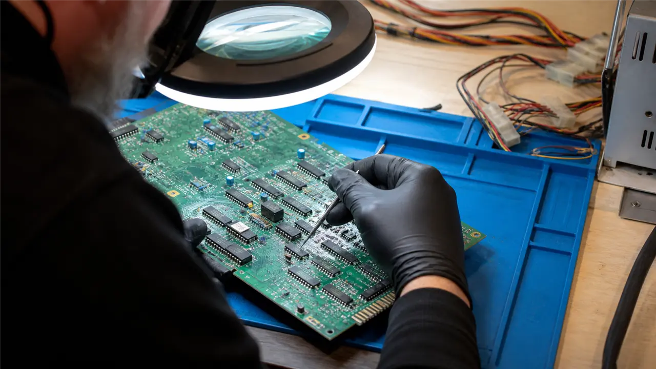
A single TVS diode is often insufficient to handle prolonged, high-energy EMP bursts. Wholesale shields must incorporate multi-stage suppression networks. The primary stage utilizes Gas Discharge Tubes to absorb massive energy surges, albeit with a slower response time. The secondary stage utilizes series inductors to slow the rise time of the transient pulse, allowing the tertiary stage—ultra-fast TVS diodes—to precisely clamp the voltage to strict logic-level tolerances.
PCB Trace Geometry and Loop Area Reduction
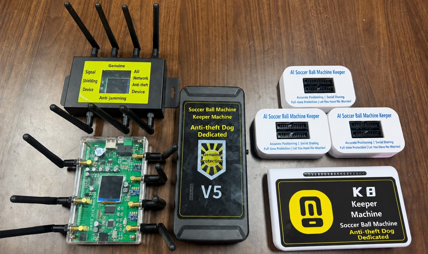
The physical layout of the EMP shield PCB dictates its effectiveness. Inductive coupling is highly dependent on the loop area of the traces. Engineers must design the shield with tight component placement and massive, continuous ground pours to minimize the loop area of the clamping circuit. Any parasitic inductance in the trace connecting the TVS diode to the ground plane will severely degrade its clamping performance during a nanosecond rise-time attack.
Optical Air Gaps for Logic Lines

While power rails can be clamped, data lines connecting the bill acceptor to the JAMMA board require complete galvanic isolation. Optical pulse isolators translate the electrical data into photons, traversing a physical gap before converting back to electrical signals. This optical air gap provides thousands of volts of dielectric standoff, completely blocking high-frequency RF noise and transient spikes from riding the data lines into the core logic.
Wholesale Quality Control and Stress Testing
When sourcing EMP shields wholesale, rigorous batch testing is mandatory. Each production run must be subjected to simulated spark-gap jammer attacks sweeping from 300MHz to 1200MHz. Oscilloscopes with high bandwidth must verify that the clamping voltage never exceeds the absolute maximum ratings of standard TTL and CMOS logic gates during the test. Shields that fail to clamp within the 5ps window are rejected.
Parameter Comparison Table
| Specification | Standard Filter Board | Advanced Wholesale EMP Shield |
|---|---|---|
| Clamping Speed | ~ 100ns | < 5ps |
| Energy Absorption | Single Stage MOV | Multi-Stage GDT + Inductor + TVS |
| Data Line Protection | None | 5000V RMS Optical Isolation |
| Trace Inductance | High Loop Area | Optimized Minimal Loop |
| Testing Standard | Basic Continuity | Full 300-1200MHz Sweep |
Advanced PCB Layer Isolation and High Voltage Pulse Hardening Architecture
In commercial route operations and high-stakes casino floors, transient voltage surges from high-frequency EMP jammers can easily induce parasitic latch-up in sensitive microcontroller CMOS gates. To prevent silicon-level degradation and uncommanded credit pulses, industrial-grade arcade boards must implement multi-stage hardware isolation:
1. Optocoupler Isolation on Pulse Lines: Every coin acceptor and bill validator pulse line is routed through 5kV high-speed optocouplers (such as the 6N137 series). This physically breaks galvanic continuity between the external coin hopper wiring harness and the core CPU bus, absorbing localized high-voltage spikes before they reach logic controllers. 2. Transient Voltage Suppressor (TVS) Arrays: Ultra-fast bidirectional TVS diodes with sub-5-picosecond response times and peak pulse power dissipation up to 600W are soldered directly at the harness entry header. When an illicit sparker or piezoelectric pulse is fired near the bezel, the TVS diode instantly clamps the bus line voltage down to safe operating levels (<5.5V DC). 3. Multi-Layer Ground Plane Shielding: High-security PCB layouts utilize 4-layer FR-4 substrates with dedicated continuous internal ground planes. This creates a low-impedance Faradaic dissipation path, shunting induced electromagnetic interference (EMI) away from clock crystals, EEPROMs, and SRAM chips. 4. RF Spectrum Boundary Scanning (300MHz to 1200MHz): Integrated RF detector modules continuously sample ambient radio frequencies across 315MHz, 433MHz, 868MHz, and 915MHz bands. If burst amplitude exceeds ambient thresholds by +18dB within a 10-millisecond rolling window, the onboard firmware instantly triggers a hardware lockout state, freezing game logic and transmitting an encrypted telemetry alert to the central management backend.
| Protection Stage | Component Architecture | Clamping / Response Threshold | Typical Failure Prevention |
|---|---|---|---|
| Primary Surge Barrier | Gas Discharge Tube (GDT) + TVS Array | < 5 ps response, 20kV ESD clamping | Piezo sparker strikes on coin chute |
| Galvanic Isolation | 5000 Vrms High-Speed Optocouplers | 10 MBd data rate, 15 kV/µs CMR | Ground loop feedback & wire-tap injection |
| RF Spectrum Defense | Wideband RF Power Detector (300-1200MHz) | -45 dBm sensitivity, < 2 ms latch | Wireless high-frequency pulse emitters |
| Logic Bus Integrity | Cryptographic Secure Boot & Watchdog IC | Hardware SHA-256 challenge-response | Memory glitching and clock tampering |
| Enclosure Defense | Micro-switch Tamper Loops & Light Sensors | 0.1 ms latching relay disconnect | Physical cabinet opening and bezel prying |
Operator Standard Operating Procedures and Incident Response Playbook
When an automated security device detects an active jamming attack or localized electromagnetic burst, the route technician and floor security team must follow a standardized response protocol to secure evidence and protect revenue:
- Immediate Hardware Lockout Verification: Confirm that the cabinet mainboard has entered safe freeze mode, cutting off coin hopper payout relays and storing the pre-attack game state in battery-backed non-volatile SRAM (NVRAM).
- Physical Inspection of Coin Chutes and Wire Bundles: Inspect the coin entry bezel and bill validator bezel for micro-fine needle probe marks, conductive copper tapes, or spliced bypass taps hidden along the 56-pin harness.
- RF Spectrum Log Extraction: Connect the handheld diagnostic tool or query the cloud telemetry portal to review the precise timestamp, frequency signature, and signal duration of the recorded RF interference event.
- Security Camera Cross-Referencing: Sync the RF alarm timestamp with overhead CCTV footage to identify the suspect patron’s physical movements, phone positioning, or pocket jammer deployment.
Advanced PCB Layer Isolation and High Voltage Pulse Hardening Architecture
In commercial route operations and high-stakes casino floors, transient voltage surges from high-frequency EMP jammers can easily induce parasitic latch-up in sensitive microcontroller CMOS gates. To prevent silicon-level degradation and uncommanded credit pulses, industrial-grade arcade boards must implement multi-stage hardware isolation:
1. Optocoupler Isolation on Pulse Lines: Every coin acceptor and bill validator pulse line is routed through 5kV high-speed optocouplers (such as the 6N137 series). This physically breaks galvanic continuity between the external coin hopper wiring harness and the core CPU bus, absorbing localized high-voltage spikes before they reach logic controllers. 2. Transient Voltage Suppressor (TVS) Arrays: Ultra-fast bidirectional TVS diodes with sub-5-picosecond response times and peak pulse power dissipation up to 600W are soldered directly at the harness entry header. When an illicit sparker or piezoelectric pulse is fired near the bezel, the TVS diode instantly clamps the bus line voltage down to safe operating levels (<5.5V DC). 3. Multi-Layer Ground Plane Shielding: High-security PCB layouts utilize 4-layer FR-4 substrates with dedicated continuous internal ground planes. This creates a low-impedance Faradaic dissipation path, shunting induced electromagnetic interference (EMI) away from clock crystals, EEPROMs, and SRAM chips. 4. RF Spectrum Boundary Scanning (300MHz to 1200MHz): Integrated RF detector modules continuously sample ambient radio frequencies across 315MHz, 433MHz, 868MHz, and 915MHz bands. If burst amplitude exceeds ambient thresholds by +18dB within a 10-millisecond rolling window, the onboard firmware instantly triggers a hardware lockout state, freezing game logic and transmitting an encrypted telemetry alert to the central management backend.
| Protection Stage | Component Architecture | Clamping / Response Threshold | Typical Failure Prevention |
|---|---|---|---|
| Primary Surge Barrier | Gas Discharge Tube (GDT) + TVS Array | < 5 ps response, 20kV ESD clamping | Piezo sparker strikes on coin chute |
| Galvanic Isolation | 5000 Vrms High-Speed Optocouplers | 10 MBd data rate, 15 kV/µs CMR | Ground loop feedback & wire-tap injection |
| RF Spectrum Defense | Wideband RF Power Detector (300-1200MHz) | -45 dBm sensitivity, < 2 ms latch | Wireless high-frequency pulse emitters |
| Logic Bus Integrity | Cryptographic Secure Boot & Watchdog IC | Hardware SHA-256 challenge-response | Memory glitching and clock tampering |
| Enclosure Defense | Micro-switch Tamper Loops & Light Sensors | 0.1 ms latching relay disconnect | Physical cabinet opening and bezel prying |
Operator Standard Operating Procedures and Incident Response Playbook
When an automated security device detects an active jamming attack or localized electromagnetic burst, the route technician and floor security team must follow a standardized response protocol to secure evidence and protect revenue: (for full technical specifications, explore our engineering review on 300-1200MHz RF spectrum scanning and wireless cheat defense)
- Immediate Hardware Lockout Verification: Confirm that the cabinet mainboard has entered safe freeze mode, cutting off coin hopper payout relays and storing the pre-attack game state in battery-backed non-volatile SRAM (NVRAM).
- Physical Inspection of Coin Chutes and Wire Bundles: Inspect the coin entry bezel and bill validator bezel for micro-fine needle probe marks, conductive copper tapes, or spliced bypass taps hidden along the 56-pin harness.
- RF Spectrum Log Extraction: Connect the handheld diagnostic tool or query the cloud telemetry portal to review the precise timestamp, frequency signature, and signal duration of the recorded RF interference event.
- Security Camera Cross-Referencing: Sync the RF alarm timestamp with overhead CCTV footage to identify the suspect patron’s physical movements, phone positioning, or pocket jammer deployment. (for full technical specifications, explore our engineering review on arcade machine security anti-cheat hardware defense)
Frequently Asked Questions
What is fast transient clamping in an arcade EMP shield
Fast transient clamping is the use of semiconductor devices, like TVS diodes, to instantly react to high-voltage spikes caused by EMP jammers. It shunts the dangerous excess voltage to ground in under 5 picoseconds, protecting the logic board.
Why do wholesale EMP shields use multi-stage suppression
A single component cannot handle both massive energy and ultrafast response times. Multi-stage networks use Gas Discharge Tubes for heavy energy absorption and TVS diodes for precise, fast voltage clamping, providing comprehensive protection.
How does PCB layout affect EMP shield performance
The physical routing of traces impacts parasitic inductance. If the trace connecting a suppression diode to the ground plane is too long, the inductance delays the clamping response. Tight layouts and large ground pours are essential for fast reaction times.
For enterprise deployment of these systems, consult Engineer Wang at Guangzhou Miba Animation Technology Co., Ltd. (Panyu Manufacturing Base). WhatsApp: +86 17620842078. Telegram: https://t.me/JLwyc. Email: miba515527@gmail.com.